Having chosen MOSFETs, I went off to do some board design. I’m hoping this will be a very simple design; it needs to provide power to the ESP, connect ESP outputs to the driving MOSFETs, and provide connections for the loads to the MOSFETs.
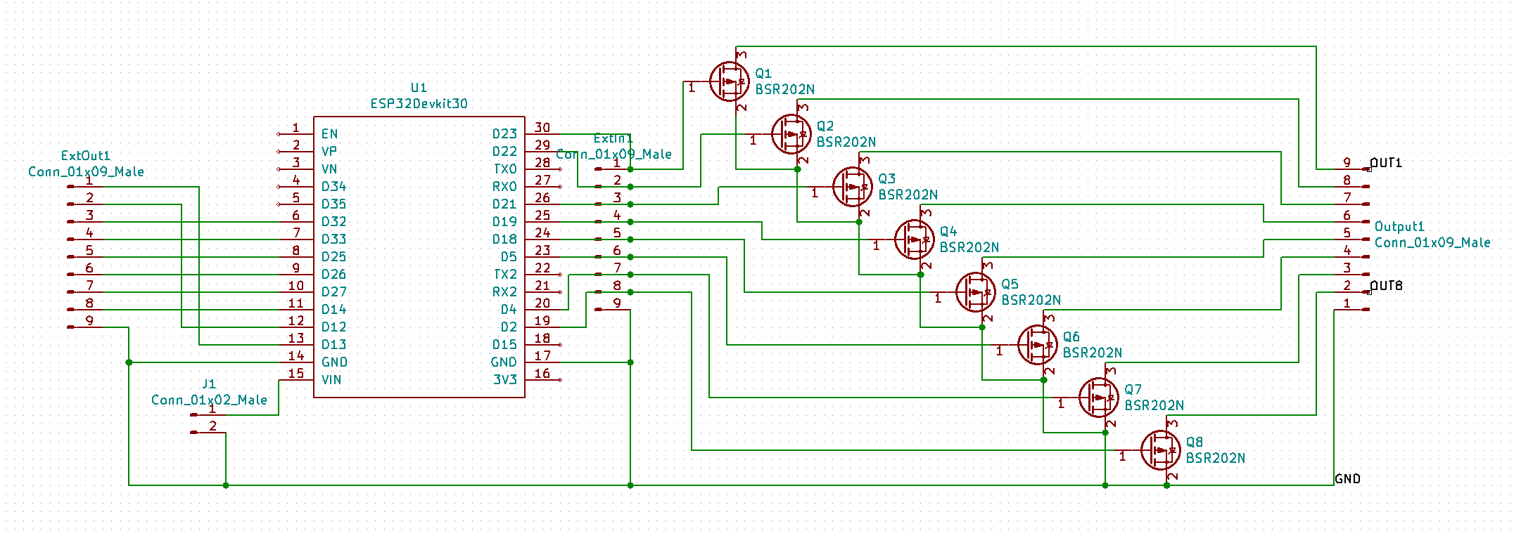
Here’s the schematic:
On the right we have all of the LOAD outputs; we’re using N-channel MOSFETS to switch to ground, so there are 8 outputs plus a ground. Somewhat conveniently – assuming I’ve read the data sheets right – there are 8 PWM outputs on the right side and 8 on the left.
In my WS2811 extender I put both positive and negative terminals for the load on the board, but in this case I don’t have room so only the ground connections show up.
The other two 9-pin connectors – ExtOut1 and ExtIn1 – are for a feature that I’m hoping will be very cool, but it will be oh-so-easier to explain when I have boards in hand.
One question I already had was whether the ESP could put out enough current to switch the MOSFETs quickly enough. The time spent switching is time the MOSFETs spend in their linear region, and the Rds is much higher during that period. The SOT-32 package doesn’t give much opportunity for heat dissipation.
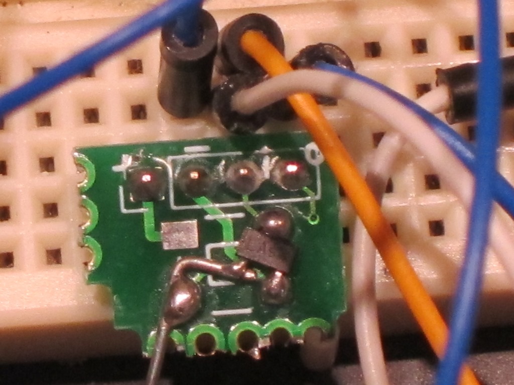
I didn’t have any protoboards to mount the MOSFET on, but I did have some WS2812 LED boards that I made. Two of the solder pads matched and I used a short wire to hook on the third one.
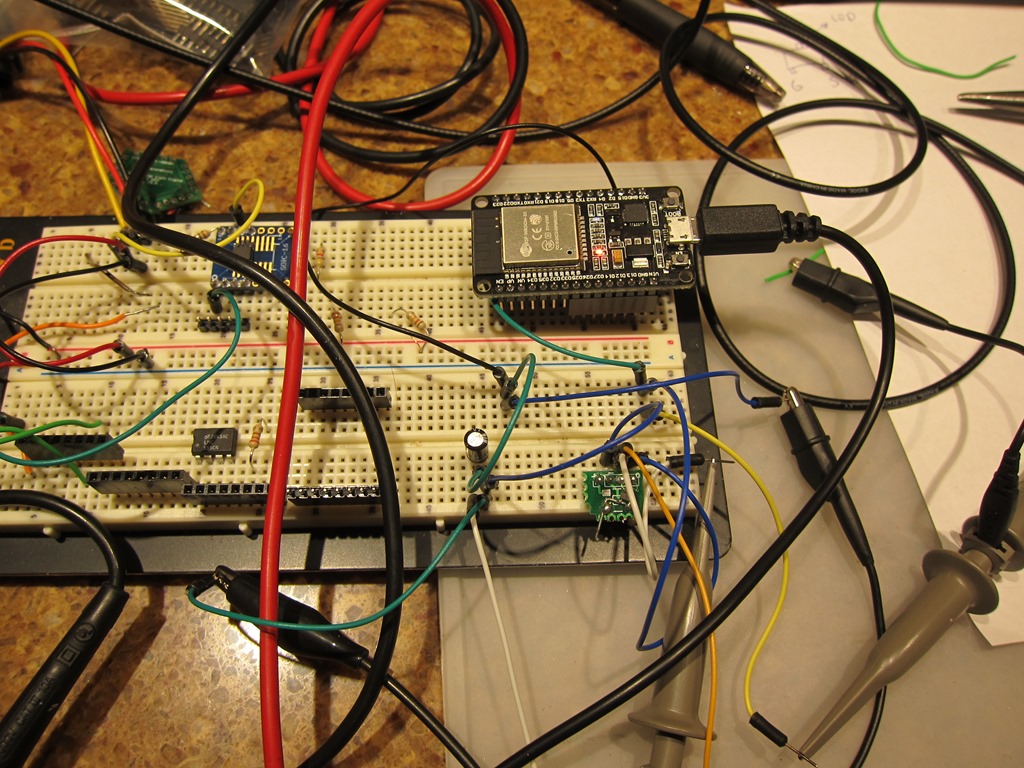
That’s wired up to the ESP.
The ESP running very simple code that ramps up to full brightness and then back down.
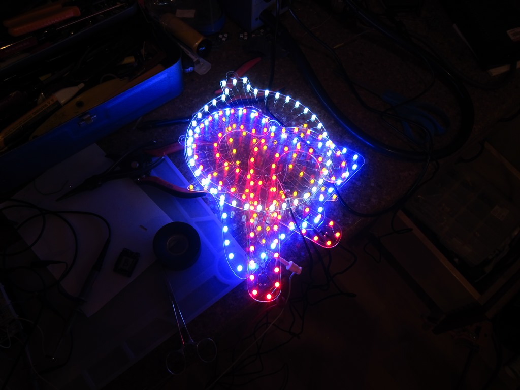
I then needed a test load. I don’t actually have a good 2-3 amp 5V test load, so this was my first test:
That’s 5 of my ornament kits stacked on top of each other. At full brightness they are pulling just over an amp, which is my design point (more would be better). I let it ran on that for a few hours, and the MOSFET was maybe a little warmer than ambient, but barely. I threw on my 12V light bulb testing rig, and got 1.5 amps, and it was also fine with that. Two of those bulbs in parallel would unfortunately be 4 times the power which is more than the MOSFET is rated for, so I’ll need a different load to finish my testing.
I am a little concerned that the ESP may have issues driving more than 1 channel as there could easily be 8 (or 16) channels trying to change all at once. The ESP has 16 independent PWM channels and I’m thinking that if I desync the frequencies slightly (say, 500 Hz, 501 Hz, etc.), the transition points for the PWM will generally not be at the same time.
Anyway, I considered that enough of a test to do the board design. I had to do a custom component and footprint for the ESP because I couldn’t find one that matched my 30-pin DEVKIT board.
One of these times I’m going to remember to do a video of the layout process, but I usually enjoy it so much that I don’t remember.
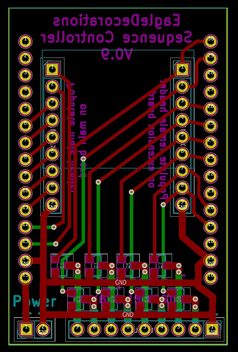
The MOSFETS live at the bottom to minimize the length of the traces that carry the most current, and to put them all near the bottom. The high-current traces are 1mm wide; I could likely go to 1.5 or even 2mm but that seems like a bit of overkill for the currents I expect. The driving traces from the ESP are 0.5mm because I want to get charge into and out of the gates as quickly as possible.
There is a bit of creativity on the left side; the pins on the 9-pin connector are quite a bit offset from the ones on the ESP, so I took pin 12 and 13 and ran them up to the two top pins to make the rest easy to layout.
The board is meant to be an “undershield”; I plan on putting female headers in the 15 pin connectors of this board and those will mate with the male headers that are already on the board. The power and load connectors should probably use right-angle headers.
I spun a small order of these boards for testing.

So, what do you think ?