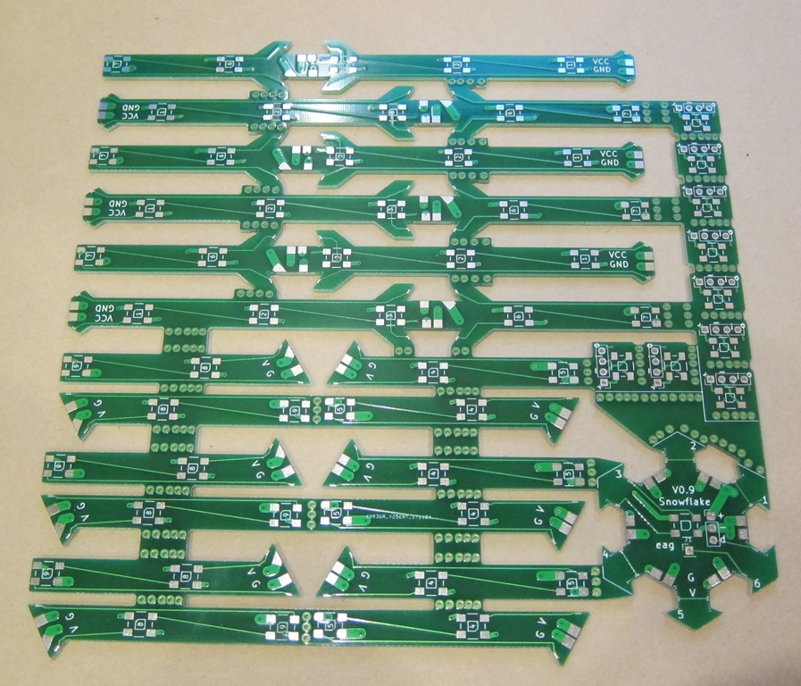
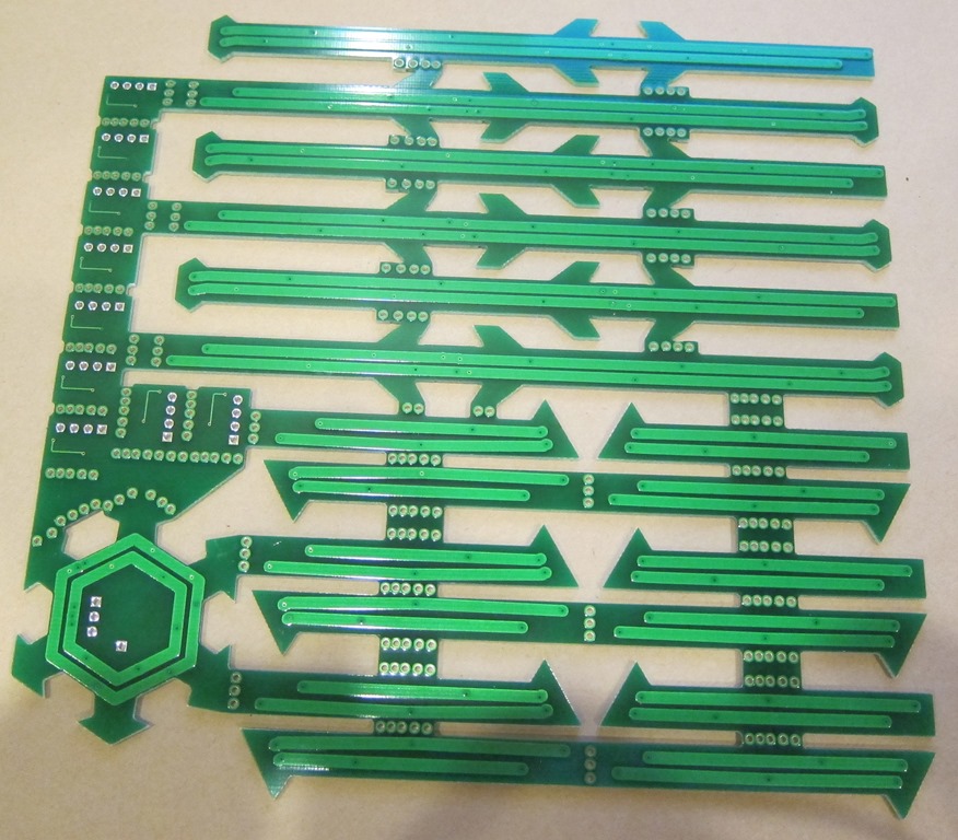
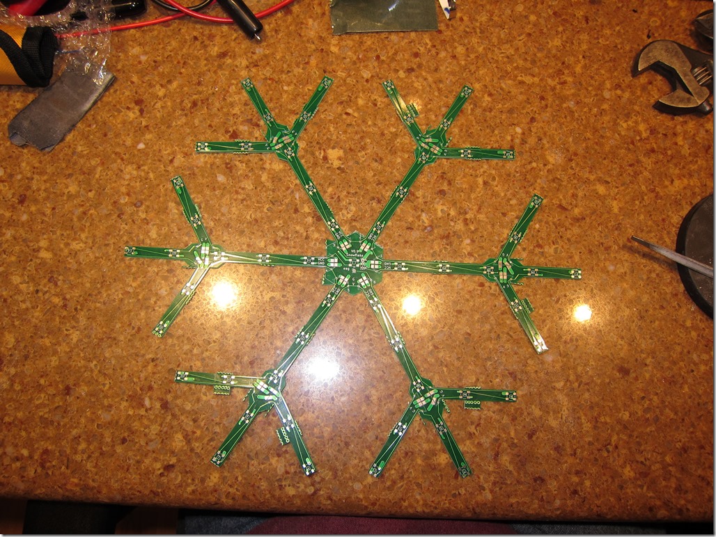
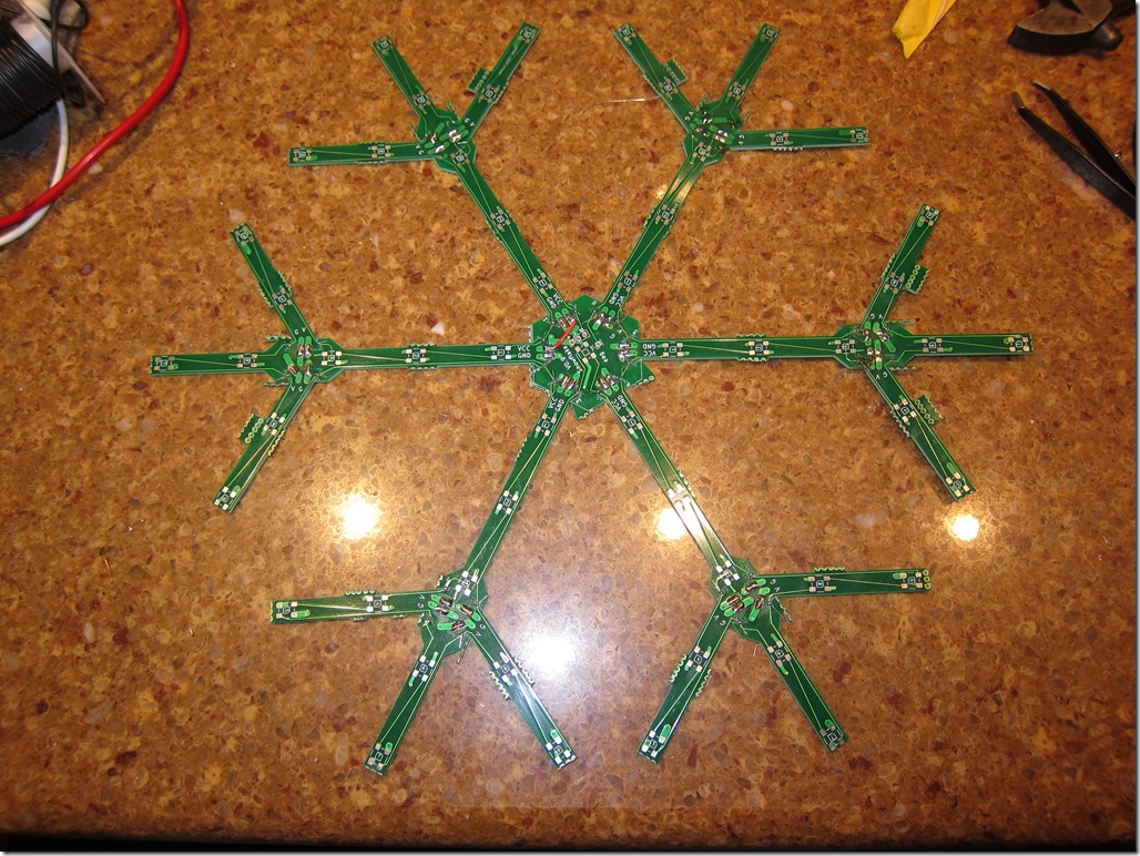
The PCBs showed up very quickly. Here are front and back pictures of them.
They look pretty nice and have holes in all the right places. Because of the design, I need to cut them apart by hand.
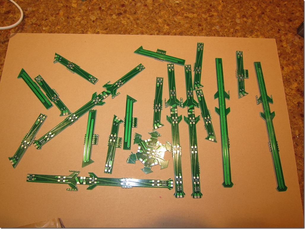
I used my Dremel osciallating multi-tool, but frankly I think the normal Dremel would be a better choice.
That gave me a pile of parts:
Next, it was time to assemble the pieces. If everything was exactly sized, all the parts should have fit together perfectly. As it was, I had a few protrusions to file down and then I needed to file most of the pieces to get them to fit together. Took about half an hour.
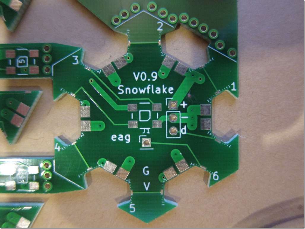
And then, the first view of the snowflake board assembled.
The *plan* was that there would be copper right to the edges of the boards, and then they could just be soldered together.
What the fab *did* was pull the copper back from the edge by a little bit, so there was a gap between each of the pads that I needed to solder together. The power and ground pads are pretty big, and I could easily bridge them with a bit of bare copper wire.
The signal lines were another matter. The pads are much smaller, and with the copper lost by the fab, I just had a hairline of pad to solder to. I ended up using very fine wires to bridge the gap, putting the super-fine tip on my Hakko, and very carefully soldering the wires on. It was pretty exacting work, but it got easier over time.
The design was perfect except for a missing via that leaves a broken connection to the Vcc line. I fixed it with a short bit of red insulated wire.
I ordered a new hot air rework station so that I can reflow the WS2812 LEDs onto the PCBs, and I’m going to use that to solder all the little jumper wires that way.
While I wait for the new tools to show up, I’m going to write some code.

So, what do you think ?